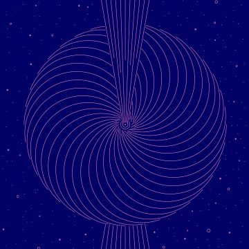
Let there be light
The material of the future is here… though chances are you’ve never heard of it. Gallium nitride has the potential to transform energy use through its incredible efficiency, and Professor Rachel Oliver has dedicated her life to the cause.
Professor Rachel Oliver has devoted her career to understanding and expanding the use of gallium nitride (GaN), yet even she was surprised at the outcome of her 2016 experiment. It was an experiment that would have potentially world-changing consequences.
“We were trying to make a quantum dot light source,” says Oliver, Professor of Materials Science in the Department of Materials Science and Metallurgy, and Director of the Cambridge Centre for Gallium Nitride. “A quantum dot gives out just one photon at a time – the smallest amount of light possible – and it can be a superb tech tool, but we were missing one component. It was seven years ago and the equipment we needed to make it was very expensive and no one would lend it to us.”
The key to the quantum dot light source was to find a way to make GaN – a highly efficient semiconductor and the core component of blue LEDs, the world’s most energy- and resource-efficient light source – more porous. GaN is made up of the soft metal element, gallium, which occurs naturally in the Earth’s crust, bonded to a structure of nitrogen atoms, grown in layers of crystals. To make it porous, you usually etch deep trenches for acid to pass through and eat holes in the material, using high-energy ions. But Oliver’s team were missing the machine that generates the high-energy ions.
I told them it wasn’t magic, it was science, and the real challenge was that we now needed to understand it
“So we made some materials and tried some other stuff to get the acid through the non-porous layers,” she explains. “It shouldn’t have worked… but it did. The acid went through the layers, without us making any holes. A member of my team was asked: ‘How is it possible?’ and he said: ‘I don’t know – it’s magic!’ I told them it wasn’t magic, it was science, and the real challenge was that we now needed to understand it.”
The team used microscopy, another area of Oliver’s expertise, to understand exactly what was going on. “People think semiconductors need to be made of extremely perfect, uniform materials, without any flaws,” explains Oliver, “whereas GaN has a lot of defects in the crystal. Everyone is always very worried about that. But what we eventually saw through the microscopes was that the defects actually created these tiny pipelines, about a billionth of a metre in size, and that’s how the acid, or etchant, was getting through. And in doing so, it also left the non-porous layer intact.”
Their discovery makes the use of porous GaN much more feasible in industrial processes, partly by simplifying the process and partly because the smooth non-porous layer increases its device compatibility. And it marks the latest stage in Oliver’s lifelong devotion to the cause. “I was always interested in the stuff around me,” she says. “Things like, why is that milk see-through? Why is that stone chilly when it’s cold, but metal is so freezing that your fingers stick to it? I was interested in concrete stuff you could touch and poke and eat for dinner.”

She settled on gallium nitride as a focus during her DPhil at Oxford. “I was interested in the mistakes in GaN,” she says, “the variations in the substructure, and how at a very small scale they can affect the properties of the material. And optoelectronics has a huge range of applications. It has the potential to have the biggest impact on global energy use.”
It’s not just about faster computers, she says, but energy and resource efficiency. “Compared to other compounds in semiconductors, GaN uses less electrical energy. The GaN blue LED, if used in its best condition, can make devices 80 per cent efficient. For comparison, a traditional ‘Edison’ light bulb is about five per cent efficient, which means about only five per cent of its electrical energy is turned into light. In a compact fluorescent bulb, the ones that take ages to come on, that rises to about 20 per cent. In a GaN lightbulb, it’s 40 to 50 per cent.”
“The pandemic showed up the fragility in the supply chain, and the UK and the US are worried about the security of it, too.”
Considering that, in the UK, we use about 20 per cent of our electricity for lighting, the potential energy savings are obvious. “In the developing world, it’s more like 40 per cent,” says Oliver. “Kerosene lamps are still much in use, and they are polluting and dangerous. Low-voltage GaN devices can run off solar power, so the energy could be stored from day to night. This means you could bring light to areas that currently don’t have it, which could have huge social impact. People could work in the day and then study at night, for example. Nobel-prize winner Hiroshi Amano, who invented blue LEDs, showed photos of Mongolian children at evening school in yurts lit by them. GaN is a social good!”
Then there’s resource efficiency. “The global supply chain for semiconductors is difficult,” says Oliver. “Materials like gallium are rare, they’re in the earth’s crust. You get gallium by mining zinc, so there’s a finite amount. Semiconductor chips are mainly made in high-tech factories in Taiwan, but they’re used inside so many devices, from phones to washing machines to cars. The pandemic showed up the fragility in the supply chain, and the UK and the US are worried about the security of it, too.”
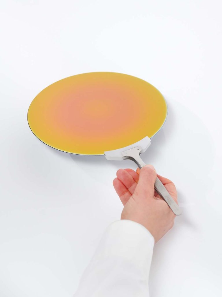
A wafer of GaN, used as the substrate for microelectronic devices used in microchips.
Oliver’s porous GaN discovery is intellectual property owned in the UK, which gives Britain a foothold in the global semiconductor supply chain. It’s also the reason Oliver has been advising the US and EU governments on their respective ‘chips’ acts, which aim to boost resilience in semiconductor technology and applications. And as the Chair of the Royal Academy of Engineering in Emerging Technologies, she is exploring how porous GaN can improve the performance of LEDs and the efficiency of the production process.
“There’s not much room to improve blue LEDs,” she says, “but if you could get amber and red to perform the same, you could have a full colour display in one system, and this would vastly improve technology like virtual, augmented and extended reality. You would be able to superimpose the internet onto everyday vision. For example, a surgeon doing an operation could access graphics and data to help make decisions through a headset without having to look away. There are obvious entertainment and leisure applications, but you could also use these screens for immersive remote work environments, so a Teams call would feel like you were sitting together in a conference room. You would be able to gesture, to have what would feel like a normal ‘in person’ interaction. This is what Zuckerberg is talking about when he refers to ‘the metaverse’.”
Oliver is also figuring how out how to retain and reuse the GaN that is discarded during the etching process. “Efficiency is about getting the most out of the crystal, as well as using less energy to make the same amount of light,” she says.
Now, she is bringing her technology to the market through her spinout company, Poro Technologies. “Equality and diversity in science and engineering is a big feature of my work,” she says. “I try and implement it in how I run my research group and my company. There are plenty of people from minority backgrounds with innovative approaches who just don’t get appreciated, so we lose people with ideas and don’t get clever science. The overwhelming majority of spinouts are founded by white men, but we are a woman and two Chinese men. People thought semiconductors had to be homogenous but it wasn’t true for GaN, and it’s not true for science either.”
Professor Rachel Oliver is Director of the Cambridge Centre for Gallium Nitride.